What is chiplets in semiconductor?
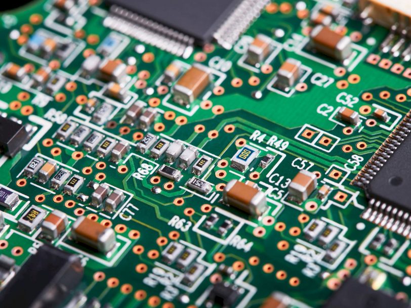
What is a chiplet? If you have come here, this is one of the questions you ask yourself. And that’s an increasingly heard term in CPU technology and also predominantly in graphics cards. It is nothing new, but it has never been as important as it is today and will continue to be so in the near future. However, this technique already has very promising successors, because it is not without its drawbacks.
What is Chiplet?
A chiplet is nothing but an integrated circuit block or chip designed to work with others similar or identical to it. In this way, a chip with a larger or more complex surface is replaced by several smaller chips.
The reason why chipsets are introduced is because the chips get bigger and it has to do with efficiency or production performance. One of its first uses for commercial processors was in 2017 by Dr. It was on AMD Zen as explained by Lisa Su.
As foundries upgraded production nodes to create increasingly smaller components, the complexity and footprint of high-performance chips increased, so costs continued to rise. Therefore, it becomes less economically viable to make larger monolithic chips. Therefore, it was decided to use chip-based designs by dividing a complex system into several smaller and simpler systems.
Note that with a die size of about 18 x 20mm that would be the middle chip, it has a surface area of 360mm², which means about 150 chips in a 300mm diameter bar. Dividing this design into four 9.5×10.5mm chipsets yields approximately 99mm², meaning that up to 622 chips can be made on one stick.
This will result in double the throughput in the second case, meaning more functional chips than in the first case. Therefore, costs can be reduced in this way. You can see it more intuitively in the image below:
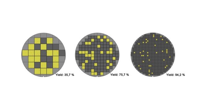
Understandably, the smaller the chip, the higher the productivity, lowering costs by producing less chip wastage and more quantity per stick. You should also take into account that Moore’s Law predicts complexity growth and the multi-core view makes the situation worse. Nodes that simply shrink cannot maintain their chip size and as a result the price goes up.
The chiplet trend goes beyond CPUs and GPUs to automotive chips, memory, etc. It seems that it will become a trend by reaching the sectors as well.
Differences with MCM
There is a type of packaging called MCM (Multi-Chip Module) that has been used for years, that is, a type of assembly that uses several chips on a substrate and is interconnected, sharing transmission pins or pads.
IBM POWER processors use the MCM package and now use AMD for their latest processors. And if you’re wondering the difference, the truth is that MCM is a term used to denote a form of packaging, and chipsets refer to chips into which a system is divided. In other words, each IC is a functional subset of the entire system and is called a chip. All grouped chips will complete the whole set.
For example, an AMD EPYC is split into chips but uses the MCM package. Intel also used this type of packaging in some cases when integrating its GPUs with CPUs, a different strategy than AMD followed in its APUs. On AMD Radeon Instinct MI200 GPUs, Intel Xe Ponte Vecchio etc. there are more uses.
As for the parts that can be seen in this type of package:
- Chiplets: These are the chips into which the system is divided. Subsystems, memory, processing units, communication units, etc. may be of various types. For example, on the IBM POWER6 in the image above, it is divided into:
- CPU cores
- Out-of-pattern L3 cache chips
- Intermediate: substrate or PCB that connects integrated circuits or chips. It is usually made from organic material. In the case of IBM POWER6 this is the brown area.
- Other: Resistors, capacitors, etc. It is also common to see surface mount components such as In IBM POWER6 you can see all the SMD components surrounding the chips.
It is interesting to note that chipsets and new packaging systems will allow the integration of interesting chips, namely heterogeneous computing, such as using various processors, memories, special accelerators such as programmable FPGAs.
The advantages and disadvantages of a chip versus a monolithic chip
Not all are advantages when it comes to MCM or chip designs, they also have disadvantages compared to monolithic designs where the entire system is integrated on a single chip. Among the advantages of chiplets:
- Minimizes design time.
- Reduces costs, increases efficiency.
- Allows you to use more memory or more processing cores. In other words, they are more scalable because they are modular.
- It provides the possibility to use several fabrication nodes on different chips and even different logic families and even different semiconductors (Si, SiGe, GaN, GaAs, InP,…).
In case of disadvantages of chiplets:
- It causes more communication delay between units.
- More complex agents are needed.
- Communication logic needs to be implemented.
- Failure to mount a pattern may mean that the entire device has stopped working.
While preserving the advantages of this division paradigm, some solutions that will try to eliminate these disadvantages of chipsets are currently being developed and commercialized. I’m talking about the new 2.5D and 3D packages where chips are stacked and you get monolith-like delays, but you can still build each stacked chip individually. An example is in 3D V-Cache, where the chips with the largest cache are placed on top of the processing units.
The problem with this type of technology is that there is still a lack of standardization, as each manufacturer uses their own methods. Therefore, if in the future it was necessary to package chips from different manufacturers in the same device, they would not be compatible. Sure Intel Foveros, Intel EMIB, TSMC LSI, TMSC CoWoS, etc. You’ve probably heard of terms like, they all have some differences…
Monolithic chips: advantages and disadvantages
Monolithic chips, just like chiplets, also have their advantages and disadvantages, which I’ve outlined here:
Advantages of Monolithic ICs:
- Smaller package size makes it more favorable for mobile or embedded devices where size matters.
- Less complexity in packaging and therefore cheaper.
- Better reliability due to fewer parts included (fewer conductor lines, welds, etc. that can fail).
- It can mean less energy consumption.
- Data transfer between different parts occurs faster and with less delay due to their proximity and because all units generally operate on the same frequency.
- Removes the need for additional logic to coordinate different chips.
Disadvantages of Monolithic ICs:
- Higher production costs than chips due to lower yield.
- More concentrated dispersion power.
- If only one transistor or interconnect fails, the entire IC stops working.
- Low flexibility and scalability.
Result evaluation about Chiplet
Although MCM chips and packaging have their advantages, some designs such as SoCs still try to remain monolithic chips as speeds have been improved. It cannot be said whether chiplets are the future of high-performance chips, rather the future will be a hybrid between different technologies.
On the one hand we will see the chips and the MCM package, which consists of stacks of integrated circuits (2.5D/3D) to bring memory and logic closer together to reduce latency, which is currently a bottleneck between CPU and RAM. In addition to all this, other technologies will come that can help improve performance even further, such as optical interconnects for much faster data transfer. It’s like switching from copper cables to fiber optics on telephone lines.
And with the emergence of silicon technology, all these technologies will become more and more important. Although some difficulties need to be solved, such as power loss when the integration level is too intense. The famous decades-old claim of “Smaller, faster and cheaper” will cost more and more.