What is lithography in CPU?
There are so many explanations about lithography in the semiconductor industry, and none of them really get the gist of it. Manufacturing nodes that manage foundries are vital to the fabrication of chips beyond the transistor density per unit area that can be integrated.
Other important factors such as consumption, construction complexity, transistor switching (respectively affecting clock frequency) also depend on the photolithographic process used.
What is lithography? & What is photolithography?
The word lithography is often used synonymously with photolithography. However, there are minor differences in terms:
- Lithography: Derived from the Greek words lithos (stone) and graphein (writing), meaning the process of writing or drawing a drawing on a stone or slab. This technique is used from ancient stone carvings to other printing procedures, etc. It can be applied in a variety of ways.
- Photolithography: As the name suggests, it is a type of lithography performed using light to transfer the pattern needed on a semiconductor surface to create ICs and MEMS.
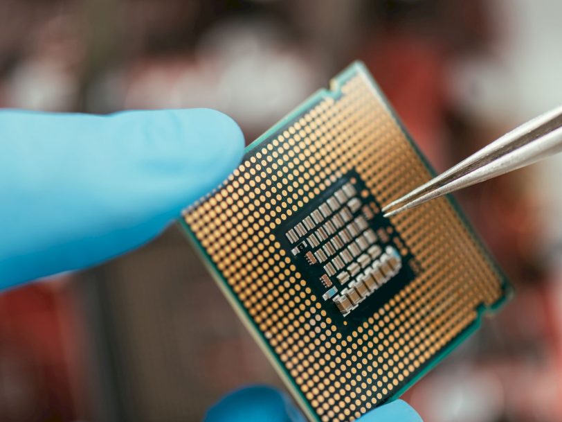
Lithography in the semiconductor industry
Photolithography or lithography is a process used in the manufacture of integrated circuits. Thanks to this technique, patterns created in a graticule or photomask can be transferred to the semiconductor surface. A photoresist is also used for this, which is light sensitive and changes its properties between exposed and unexposed areas. In this way, it can be used as a mask for other operations that you want to affect only a certain area.
Masks are usually made of quartz and chrome, others use other materials such as sapphire, glass, and other metals other than chromium. The glass parts are the parts that allow light to pass, and the metal parts are the parts that will create shadows. Of course, these masks are much larger than the patterns to be engraved on the chips, but they are scaled down by a very complex optimization system.
During the lithography process, some basic steps are usually performed, such as:
- Application of the resin to the surface. This is done using a spinner or machine that spins the rod at high RPM and another robotic machine that pours the liquid resin onto the rod. This ensures that the resin is applied evenly over the entire surface and removes the excess.
- The next step is to pass the rod through an oven and gently heat it to fix the resin to the semiconductor substrate.
- Then comes the exhibition. To do this, the mask (with patterns to be projected such as transistor wells, gates, interconnects, etc.) is placed between the light source (lamps, lasers, electron beams,…) and the sheet. Transparent areas that allow light to pass through change the resin, while shadow areas prevent light from intersecting with the resin.
- Now comes the chemical attack, this is the step where the exposed or unexposed area (depending on the positive or negative resistance type) is eliminated by means of an acid bath.
- And finally comes the process necessary to produce what is intended to be created. For example, metal deposition to create interconnections in non-photomask areas, ion implantation in semiconductor (N or P) dope fields, oxidation to form insulators, digging “ditches” in the substrate for FinFETs, etc.
- After that, the non-removable photo mask can be removed. It has already fulfilled its mission and has prevented the previous process from affecting areas where engraving was not intended.
These steps are repeated over and over until the entire pattern of the integrated circuit intended to be created, that is, the physical implementation of the microarchitecture, is completed. Some processes need several dozen different masks to create everything from transistors on the semiconductor substrate, to the first interconnect layers that weave transistors together to form logic gates or memory elements, to the middle and upper layers that will weave all those foundations.
Before concluding this section, I would like to talk about the lighting technologies used in photolithography. Light sources vary and are important to the node as they determine the wavelength of the electromagnetic beam, from visible light to some colored lights, UV and even other low wavelength radiation. Two main technologies are currently used:
- DUV (Deep UltraViolet): Using deep UV, this technique has light wavelengths between 248 and 193 nm, allowing details down to 50 nm. The technique to reduce this size is 193 nm light and different liquids, OPC, PSM, etc. can be developed using immersion lithography. Some recent DUV applications have managed to reach 157nm and render less detail than 32nm.
- EUV (Extreme UltraViolet): Included in a more advanced technique known as nanolithography, which can use even lower resolutions. It relies heavily on receiving UV radiation to achieve very short wavelengths of the order of 13.5 nm using techniques such as NGL. EUV is currently used for the manufacture of memory chips, CPUs, GPUs, among others.
- NGL (Next Gen Lithography): Next generation lithography, electron beams (eBeam) instead of light, ion lithography, X-rays etc. It covers some other nanolithography procedures using Thanks to them, even EUV can be improved.
Note that the lower the process, the higher the resolution for device fabrication, which will translate into smaller components. For example, a 7nm node does not mean that the transistor is 7nm, but details of these dimensions can be formed.
Importance of a chip's lithography
Why would you invest so much money to shrink the nodes and create components that are smaller and smaller in nanometers? Maybe it’s a question some people ask. And the answer isn’t that chips are getting smaller (in fact, with advanced chips the trend seems to be the opposite, they grow in unit area), it’s quite different. Lithography needs improvement because such critical factors depend on it:
- Size-complexity: If all parts of a transistor are shrunk equally, the electrical properties of that transistor will not change, but more transistors can be created per unit area, meaning that more complex chips can be produced with better performance. For example, more execution units, larger memory size, more functions, etc.
- Capacitance switching: Smaller transistors also have lower capacitance, allowing them to switch from one state to another more quickly, leading to the possibility of increasing the clock frequency.
- Capacitance-consumption: On the other hand, lower capacitance can also change with less power, which translates into more energy efficient chips. In short, dynamic power, ie non-static power, will be less consumed when transistors are not idle.
- Surface costs: smaller chips also mean lower production costs and better yields per wafer. The more the lithography node or process is reduced, the less surface the same design takes up so that more can be produced per wafer.
Unfortunately, there are also disadvantages to increasingly reducing the size of transistors:
- Defect-yield: the smaller it is, the more difficult it will be to control the production processes at this small scale, hence the greater the defects. Therefore, binning allows some or all features that cannot be labeled with maximum speed to be used in a way that does not affect the efficiency much. Techniques such as the chiplet have also been created to alleviate these problems.
- Leakage: The smaller the transistors, the more leakage. That is, there is more current flowing through the transistor and wasted when it is off. Therefore, while dynamic power decreases, static power increases if nothing is done to mitigate this effect. To solve this, some techniques have been developed such as SOI, new materials, new structures, among others.